LECTURE 7: Microprocessor Structure, Assembly Programming
Microprocessors
Earlier computing systems were classified into mainframes, mini-computers, and microcomputers. The microcomputers were desktop machines, supporting a single user. The "brain" of a microcomputer was a single IC (integrated circuit) chip. It is usually called the CPU (central processing unit).
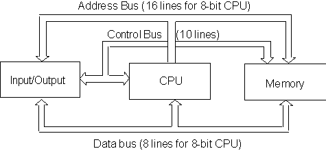
All operations performed by the computer are in the form of a set of simple instructions which are held in the computer memory. The CPU extracts these instructions from the memory, and executes them in order. The structure of the simplest microprocessor is shown in fig 7.1

Figure 7.1. The architecture of a microprocessor
The CPU
Figure 7.2 shows the internal organization of a simple CPU. The various blocks show a logical break-down of the functions performed by the CPU, and the arrows show the flow of data between these functions.
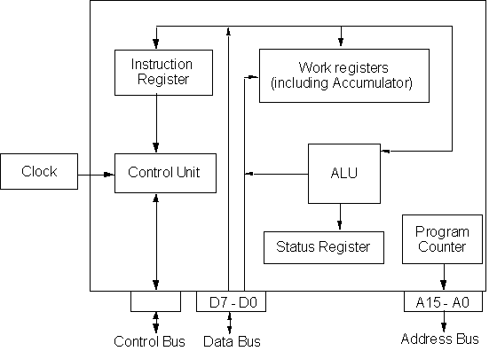
Figure 7.2. Internal organization of the CPU
The registers are used to store binary information during the execution of a program. Each register has a specific function associated with it:
The Accumulator is the primary register associated with the ALU and the input/output operations. At the beginning of the ALU operation, one operand (data value) is taken from the accumulator while the second operand is taken from the memory. The resultant value, after the operation is complete, is stored in the accumulator.
The instruction register holds the binary code of the instruction that is being executed.
The program counter contains the address of the memory location from which the next instruction code will be taken.
The functional units of the CPU are:
The timing unit, composed of an internal clock (which is basically a small chip oscillating at high frequency by application of a voltage, and associated hardware that result in a pulsed wave form voltage as shown in figure 7.3). With each pulse of the clock signal, an electronic switch is activated that causes the next (most elementary) step in the execution of the processor gates. It can therefore be seen how the clock frequency is related to how fast a microprocessor operates (although, as we learn more details, we shall see how the speed of the processor as perceived by the user can depend on many other things also.)

Figure 7.3. The output of the clock
The control unit is composed of a controller-sequencer and an instruction decoder. During execution, the control unit causes the contents of the program counter to be placed on the address lines. These lines now indicate the address of the memory location containing the code of the next instruction to be executed. Next, the control unit causes the instruction code to be transferred into the instruction register. The instruction decoder is now enabled and the control unit can activate the necessary control lines to cause the desired results. For example, suppose the contents of the memory location following the instruction code is to be added to the contents of the accumulator. The control unit will increment the program counter and obtain the desired address (of the data value which is in the memory), enable the address bus with the new address, and then transfer this data to the ALU. Next, the control unit will transfer the contents of the accumulator to the ALU. The ALU performs the necessary instruction (in this case, addition), and updates its status register. The control unit then transfers the result from the ALU to the accumulator. This completes one instruction cycle.
The Arithmetic and Logic Unit (ALU) is the part of the processor which actually performs the basic arithmetic or logic operation on the data.
Memory
All information in a computer is stored in memory. The physical medium of storage are varied - chips, tape, discs. Most of the microprocessor memory is on chip since it allows faster access. Examples of memory types are:
Memory types:
ROM (example? ):
PROM (programmable ROM):
EPROM: erasable PROM, which can be erased by UV-light and reprogrammed
RAM:
The memory circuit of the microprocessor is shown in fig 7.4.

Figure 7.4. A Simple microcomputer memory chip
Note that the CPU is connected to the RAM via a Read/Write line, but not to the ROM. Why ?
The 'CS' switch is the Chip Select line, which has to be enabled for the contents of the address in the memory to be loaded on the data bus.
The address bus carries the binary address of the memory location to be accessed. In the example shown above, it is made up of 11 lines. Each address has one byte (8 bits) of data, which are transferred to (or, in case of write operations, from) the CPU via the data line. How many bytes of memory are available on the chip ?
How many bits ?
Input/Output:
I/O chips are used to connect the microprocessor to a variety of devices (called peripherals). The most common of these include memory disks, printers, data-links to other computers (forming networks), instrumentation controlling equipment, etc.
The most common of I/O chips are either Parallel Input/Output (PIO), Serial I/O (UART, or Universal Asynchronous Receiver/Transmitter), CTC (Counter Timer Circuit) and FDC (Floppy Disk Controller).
You will often find descriptions of computers telling you how many parallel-ports and serial-ports it provides. This gives you an indication of how many peripherals you can attach directly to your computer.
PIO: The PIO chip passes data through 8 pins (or lines) between devices. A typical PIO chip schematic is shown in Figure 7.5.

Figure 7.5. Parallel I/O chip, pin functions
The two address bus lines are used to provide four addresses on the PIO as follows:
0 0 : Port A
0 0 Port B
1 0 Port C
1 1 Control register
The control register is used to control the direction of the ports (input or output).
UART: serial ports.

Figure 7.6. UART pin functions
The serial port transfers data between devices in much the same way as a parallel port, except that in this case, there is a single wire over which data is communicated. Thus the 8 bits in each byte are first converted into a series of pulses, and then transferred. A clock pulse signal is required to trigger the transfer of the 8 serial data bits whenever a byte is transferred. The cabling for this mode is cheaper, but the data transfer rate is much slower.
CTC:
A CTC is a programmable counter that can be loaded and read back to the CPU. Three of the most common applications of CTCs are : pulse generator, real-time clock interrupt, and external event counter. In the pulse generator, the counter automatically reloads itself once the count reaches zero; thus a regular stream of pulses is generated. As an interrupt, the interrupt signal is generated which causes the CPU to execute a special interrupt program. This program can update counts in memory that represent the time-of-day, and other programs can either use this time-of-day clock or can be called at specific times. As an external event counter: software can be used to read the count, or to reset it to zero; this is a very efficient way of counting external events, which would otherwise have to be recorded using interrupts each time such an event occurred.
Why is a clock so important in a computer ?
How does it regulate the activities of the CPU ?
How is the clock signal generated ?
What is a counter ? How is it useful (relate to one used in the PLC's )?
FDC (Floppy Disk Controller):

Figure 7.7. Floppy Disc Controller pin Functions
The floppy disc is a device familiar to anyone who has worked on personal computers. The most common format of the floppy is the 3.5" discs with the hard plastic shell and sliding metal window. The actual data is stored on a thin plastic sheet which is coated with magnetic material. Reading or writing data from the floppy is done by a device called the "head" (similar to audio cassette player heads). The data storage is via magnetization of a small portion of the disc by application of a magnetizing field generated by passing current through a coil in the head. Reading of the data is performed by sensing the induced voltage in the read head as it is passed over a magnetized area.
The data is arranged on tracks (e.g. in the older floppies, 77 concentric tracks, 24 sectors per track, 128 bytes per sector). How many Kilobytes is that ?
How much data can you store on a floppy disc now ?
A typical transfer procedure for a disc write operation is as follows. Software loads the track register and sector register with the required position on the disc where the data is stored. The FDC moves the head assembly to the desired track by pulsing the stepper motor, and waits until the disc has rotated until the required sector is beneath the head. The head is then "loaded", or brought close to the disc. An interrupt signal is generated, upon receipt of which, the software loads the data register with the data byte that is to be written. This byte is then transferred to the read/write head (activated to "write") in serial form. The data transfer is continued till all data has been transferred to the disc.
Most modern computers also have a "hard" disc, which is typically made of a metal disc, and rotates at a very high speed (allowing much faster data access than a floppy, for instance). Hard discs are designed for file storage on the computer, and are therefore RAM. The data access off a hard disc is similar to that of a floppy disc. The physical structure of hard discs is shown in figure 7.8.

Figure 7.8. A moving-head hard disc system
Microprocessor Programming:
With the structure described above, how exactly does the microprocessor work ? How, in other words, does a computer perform the various tasks it is supposed to ? It does this by:
(1) knowing how to perform a set of very simple tasks.
(2) having a protocol to orchestrate the functioning of all devices connected to the CPU.
The set of simple tasks that the processor can perform are called the instruction set. The instruction set is usually composed of two parts: the first part is a mnemonic called the opcode, which tells what the processor is supposed to do. The second part, which may be composed of one or two words, contains either data, or addresses where data manipulation is to take place. The actual values of these words depends upon the opcode, as will be seen from our simple instruction set below. Usually, the arguments (data) which each opcode operates on is called operand(s). The entire instruction set and its syntactic rules form a grammar that the CPU can understand and act upon. It is called assembly language. We shall deal with a hypothetical, small assembly language. Actual assembly languages have larger instruction sets, since real computers perform more sophisticated tasks than the ones we shall simulate. Also, mainly for the sake of simplicity, we shall use an over-simplified model of memory. We shall refer to any address in memory by a label. Labels can have any decimal numeric value (positive integers, of course).
The instruction set of out pseudo-assembly language, and its descriptions are as follows:
OPCODE OPERANDS Description
LDI r N Load Immediate. Load register r with number N
LDR r addr Load Register. Load register r with contents of memory at location addr
MRR r1 r2 Move between registers. Copy contents of register r1 into register r2. Current value of r2 is overwritten
MRM r addr Move from register to memory. Copy contents of register r into memory at address addr
JMP addr Jump unconditional. Jump to memory address addr. Program counter is set to addr
JEQ addr N Jump if equal. Jump to memory address addr if the contents of Accumulator (register A) equal N
JNE addr N Jump if not equal. Jump to addr if contents of accumulator ≠ N
ADD r N Add. Add N to contents of register r
SUM N1 N2 Sum direct. Add N1 and N2, place result in Accumulator (register A)
ARR r1 r2 Add contents of registers r1 and r2, place result in Accumulator
SUB r N Subtract. Subtract N from contents of register r
DIF N1 N2 Difference direct. Put result of N1 - N2 in Accumulator (register A)
SRR r1 r2 Subtract contents of register r2 from the contents of r1. Result in register A
DEC r Decrement contents of register r by 1.
INC r Increment contents of register r by 1
AND N1 N2 Compute bit-wise AND (logical AND) of the binary equivalent of N1 and N2; put result in Accumulator
ORR N1 N2 Compute bit-wise OR of N1 and N2
XOR N1 N2 Compute bitwise XOR of N1 and N2
HLT Halt. This is the last statement executed in any program.
To understand how the microprocessor works, we shall go through a small example program on our hypothetical microprocessor. Our microprocessor has 8 bit registers. This imposes restrictions on its functioning:
1. What is the largest number that can be represented using 8 bits ?
2. How about negative numbers ?
3. How are opcodes, registers, and operands distinguished ?
In practical terms, how does this affect our simple microprocessor ?
1. The memory is limited to a maximum of 0.1K bytes (0-99).
2. The microprocessor can handle a maximum of double digit numbers (-99-99).
Despite these limitations, this simple microprocessor is in fact quite similar to the Intel™ 8086 microprocessor, which was one of the most popular chips on small computers.. a stepping stone to the Intel™ 80486 chips which are the processors on the computers you see all over the HKUST campus.
Example:
LDI A 10
ADD A 7
HLT
This simple program adds the numbers 10 and 7. The first step, before the program can be executed, is to load the program into memory. For the time being, let us assume that the program can be loaded into memory from the top (memory address 0), which is where the microprocessor shall begin execution. In real microprocessors, the top of the memory space is used for microprocessor controlling programs (called operating systems), and user programs are loaded in separate memory locations and executed from there. The principle of the operation remains the same, however.
The execution of the program is shown pictorially in figs 7.9-7.22.

Figure 7.9. Starting the execution. The Fetch Phase

Figure 7.10. The fetch Phase: setting the Address Register

Figure 7.11. The fetch Phase: Accessing the Memory

Figure 7.12. Completing the fetch phase

Figure 7.13. The execute Phase: Instruction decoding

Figure 7.14. Fetching the operands
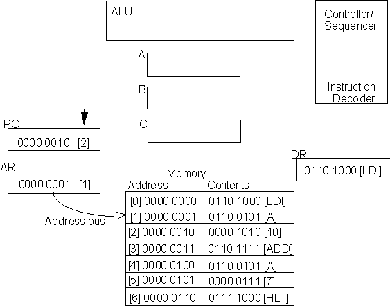
Figure 7.15. Transfer of the first operand

Figure 7.16. Identification of first operand
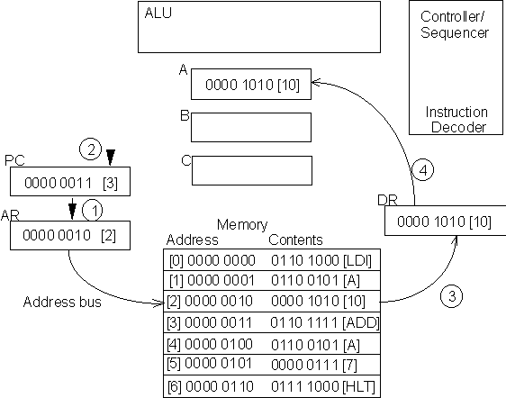
Figure 7.17. Transfer of the second operand

Figure 7.18. Fetching/Identifying the next instruction

Figure 7.19. Transfer and identification of the first operand

Figure 7.20. Transfer of data into ALU for computation

Figure 7.21. Output of result to the prescribed register

Figure 7.22. Fetch, Identify, Execute the final instruction.
Modern microprocessors are much more complicated than this simple model. They provide a much larger instruction set, much larger memory, 16-, 32- or even 64-bit registers, and many other functions. However, the basic principles of the operation of the microprocessor unit remain, in an abstract sense, very much the same as presented here.